A Method and Flow of DRAM Wafer Testing Using Test Pin Card
The invention relates to a method for performing DRAM wafer testing using a test pin card.
Background technique:
DRAM has the need to reduce test costs during the testing process. Therefore, the same number of test needle cards is getting higher and higher, and the manufacturing cost and maintenance cost of test needle cards are also increasing accordingly.
Take the test pin card of the same test with 256 chips as an example. The price of a needle card is $200,000, and the cost of repairing a test probe is $1,000.
The traditional DRAM wafer test method is shown in Figure 1. The test is performed in three steps:
Step 1: Wafer starts;
Step 2: Functional testing, that is, performing various functional test items of the DRAM;
Step 3: The test ends.
The protection of the test pin probe is not taken into account in conventional DRAM wafer testing. According to the above test procedure, when the test abnormality occurs, the test probe is easily damaged, and the damage of the probe further leads to the lag of mass production and the increase of the cost of the chip.
Technical realization elements:
The invention improves the process of the traditional DRAM wafer test by using the test pin card, and proposes a new test method, which can avoid the mass production lag and reduce the chip cost as much as possible.
The test scheme of the present invention is as follows:
Step 1: Wafer starts;
Step 2: Determine the key probes in the test needle card that need to be protected, and then separately test the test items related to the key probes;
If a test item fails, the corresponding failed chip power supply is turned off, and then the next test item is continued for other chips until all the test items are completed;
Step 3: Functional testing, that is, performing various functional test items of the DRAM;
Step 4: The test ends.
At present, there are two main types of key probes for DRAM mass production test card.
That is, the power probe (VDD and GND) and the probe that controls the chip characteristic voltage (VPP, VNWLL, etc.), because these two types of probes will flow with high voltage or large current during the test. Therefore, the two types of probe chips cannot be shared, and it is important to protect these two types of probes.
Therefore, the key probes that need to be protected usually include the power probe and the probe that controls the characteristic voltage of the chip. The test items for the key probes in turn include: Short-circuit test for VDD and GND, IDD1 test for VDD current clamp, DC test for high voltage at characteristic voltage.
The beneficial effects of the present invention are as follows:
The key probe of the DRAM test pin card is effectively protected, and the mass production lag caused by the abnormality of the test pin card is avoided, and the cost of mass production is also reduced.
FIG 1 is a flowchart of a conventional DRAM wafer test.
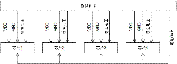
FIG.2 is a schematic diagram of a test pin card and a chip connection of a 4-chip test.
FIG.3 is a flow chart of the DRAM wafer test of the present embodiment.
Technical characteristics:
1. A method for testing a DRAM wafer using a test pin card, including
Step 1: Wafer starts;
Step 2:
Determining the key probes in the test needle card that need to be protected, and then separately testing the test items related to the key probes; If a test item fails, the corresponding failed chip power supply is turned off, and then the next test item is continued for other chips until all the test items are completed;
Step 3: Functional testing, that is, performing various functional test items of the DRAM;
Step 4: The test ends.


Background technique:
DRAM has the need to reduce test costs during the testing process. Therefore, the same number of test needle cards is getting higher and higher, and the manufacturing cost and maintenance cost of test needle cards are also increasing accordingly.
Take the test pin card of the same test with 256 chips as an example. The price of a needle card is $200,000, and the cost of repairing a test probe is $1,000.
The traditional DRAM wafer test method is shown in Figure 1. The test is performed in three steps:
Step 1: Wafer starts;
Step 2: Functional testing, that is, performing various functional test items of the DRAM;
Step 3: The test ends.
The protection of the test pin probe is not taken into account in conventional DRAM wafer testing. According to the above test procedure, when the test abnormality occurs, the test probe is easily damaged, and the damage of the probe further leads to the lag of mass production and the increase of the cost of the chip.

Technical realization elements:
The invention improves the process of the traditional DRAM wafer test by using the test pin card, and proposes a new test method, which can avoid the mass production lag and reduce the chip cost as much as possible.
The test scheme of the present invention is as follows:
Step 1: Wafer starts;
Step 2: Determine the key probes in the test needle card that need to be protected, and then separately test the test items related to the key probes;
If a test item fails, the corresponding failed chip power supply is turned off, and then the next test item is continued for other chips until all the test items are completed;
Step 3: Functional testing, that is, performing various functional test items of the DRAM;
Step 4: The test ends.
At present, there are two main types of key probes for DRAM mass production test card.
That is, the power probe (VDD and GND) and the probe that controls the chip characteristic voltage (VPP, VNWLL, etc.), because these two types of probes will flow with high voltage or large current during the test. Therefore, the two types of probe chips cannot be shared, and it is important to protect these two types of probes.
Therefore, the key probes that need to be protected usually include the power probe and the probe that controls the characteristic voltage of the chip. The test items for the key probes in turn include: Short-circuit test for VDD and GND, IDD1 test for VDD current clamp, DC test for high voltage at characteristic voltage.
The beneficial effects of the present invention are as follows:
The key probe of the DRAM test pin card is effectively protected, and the mass production lag caused by the abnormality of the test pin card is avoided, and the cost of mass production is also reduced.
FIG 1 is a flowchart of a conventional DRAM wafer test.
FIG.2 is a schematic diagram of a test pin card and a chip connection of a 4-chip test.
FIG.3 is a flow chart of the DRAM wafer test of the present embodiment.

Technical characteristics:
1. A method for testing a DRAM wafer using a test pin card, including
Step 1: Wafer starts;
Step 2:
Determining the key probes in the test needle card that need to be protected, and then separately testing the test items related to the key probes; If a test item fails, the corresponding failed chip power supply is turned off, and then the next test item is continued for other chips until all the test items are completed;
Step 3: Functional testing, that is, performing various functional test items of the DRAM;
Step 4: The test ends.
