Anti-electromagnetic Interference Design of Metal Shell
1. EMI (Electro Magnetic Interference) is electromagnetic interference. The mode of transmission is radiation and conduction.
2. Important regulations:
FCC ( Federal Communication Commision) in the United States
VDE (Verband Deutscher Electrotechniker) in West Germany
CISPR (Comite International Spe Ciai Des Perturbationss Dadioelectriques) of the IEC (International Electrotechnical Commission)
3. Degree of control
Commercial products must comply with Class A.
General household use to comply with Class B
4. Countermeasures against electromagnetic interference
Parts Selection _ Appropriate electronic parts can be reduced by 2~3dB
Circuit Layout_ Board Pattern Design Change
Noise FILTER_ power supply noise can be taken 1 OW PASS FILTER
Grounding _ The principle of multi-point grounding for high-frequency circuits
CABLE_ with shielded CABLE
Connector_ with a shielded Connector
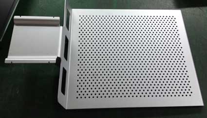
Housing _ Metal shell, plastic shell surface conductive material treatment: Non-electrolytic plating, ZINC SPRAY, aluminum evaporation, conductive paint spraying, and metal foil attached or directly formed with conductive plastic.
5. Conductivity must be considered
Temperature, humidity, aging and Impact test, adhesion test shall comply with the provisions of UL746C, the result is above 4 (peeling within 5%)
6. Definition of surface resistance
Specific resistance Rr=△V/I * S/ l
Resistance Rs=Rr/t (Ω)
7. Shielding effect
Screening effect of electric field SdB=20 log E1/E2
Magnetic shielding effect SdB=20 log H1/H2
Where E1, H1 is the incident wavelength intensity, E2, H2 is the penetration wavelength intensity
Shielding Effectiveness
SE=R+A+B
R: reflection attenuation: R=168+10log(c/p * 1/f)
A: Absorption attenuation: A=1.38 * t√f*c*p
B: multiple reflection attenuation: usually negligible
Where c is the relative conductivity, f is the frequency, p is the relative permeability, and t is the thickness of the shadow.
|
material |
Relative conductivity (C) |
Relative magnetic permeability (P) |
C * P |
C/P |
|
silver |
1.05 |
1 |
1.05 |
1.05 |
|
copper |
1.00 |
1 |
1.00 |
1.00 |
7. Anti-electromagnetic interference design
If the shielding layer has openings such as holes, the shielding current will be affected. In order to make the current smooth, the long hole can be changed into a plurality of small round holes.
Shields with aligned holes are affected by several factors
The maximum diameter d of the hole, the number of holes n, the hole spacing c, the shielding thickness t, the distance r between the noise source and the hole, the frequency f of the electromagnetic wave, wherein d, n, f are as small as possible, and the larger c, t, r is, the better.
The relationship between the indirect seam of the shell and the shielding effect
1. Conductive contact must be maintained, so do not spray non-conductive paint.
2. The seam overlap width is 5 times larger than the seam.
3. The distance between conductive contacts is less than λ/20~1.5cm
The radiation generated by an electromagnetic field is composed of an electric field and a magnetic field, but the influence of the magnetic field on health is considerable.
Electric field radiation can block, but magnetic field radiation can penetrate most of the material, including cement and steel.
The magnetic field strength of general household appliances is below 5 milli Gauss (1mG=100nT)
8. Anti-electromagnetic material
Different materials and material thickness have different effects on frequency absorption. The absorption loss of iron of the same thickness is greater than the absorption loss of copper.
9. How to suppress electromagnetic interference
First of all, we must clearly understand what specifications are required, and the frequency bands and levels that are limited by each specification are different. The countermeasures are not the same.
To suppress the occurrence of EMI, it is first necessary to suppress the source of its occurrence, and then try to prevent it from being induced to become its propagation, radiating the antenna I/O. On the power cable, and to avoid signal cables and data passing near the gap of the frame, this can reduce the direct radiation of the circuit and the secondary radiation from the gap between the cable and the frame.
Radiation from digital devices has differential and common modes
1. Differential mode radiation --- This is due to the high frequency current flowing in the loop formed by the circuit conductor, which acts as a small antenna for the radiated magnetic field.
This signal current loop is necessary in the circuit operation, but to suppress the radiation, it must be limited in size during the design process.
In order to suppress radiation, printed circuit boards must minimize the area of the loop formed by the signal current. The entire trajectory of the high-frequency (>500 kHz) periodic signal is found on the circuit diagram, the path is configured as short as possible, and the shunt capacitor is individually arranged near the component that drives the high-speed periodic trajectory.
Common mode radiation--- When the common mode potential of a certain part of the system is higher than the true ground potential, when the external cable is connected to the system and driven by the common mode, the antenna of the radiated electric field is formed. The common mode radiation is determined by the common mode potential from the radiated frequency of the circuit structure or cable, which is different from the differential mode signal of the cable.
The reduction of the common mode radiation is the same as in the differential mode. It is best to suppress the rise time and frequency of the signal. In order to reduce the radiation designer can control only the common mode current.
1) Minimize the source voltage (usually the ground voltage) of the drive antenna
2) Insert the common mode choke in series in the cable
3) Short circuit current to ground (system ground)
4) Shielded cable
The first step of suppressing the common mode radiation is to minimize the common mode voltage of the driving antenna. Many methods of reducing differential mode radiation can also reduce common mode radiation.
When selecting electronic components, be careful to select components that have the necessary minimum rise time.
If the clock speed is reduced by half, the amplitude of the harmonic will drop by 6dB. If the rise time is doubled, the amplitude will drop by 12dB. Obviously, slowing down the rise time is an effective means to suppress the source of noise.


